


Research
Condensed matter physics is a fascinating branch of physical sciences that allows us to study and understand the matter that surrounds us. One particular category of matter, namely semiconductors, have revolutionised our life as their integration into electronic and optoelectronic devices facilitated the development of numerous technological advances. The vast majority of these devices are based on crystalline, highly ordered systems such as Si and GaAs, the physics of which is well understood after extensive research over the last seven decades. Additionally, these devices begin to reach the limits of their potential performance as exemplified by Moore’s law and the Shockley–Queisser limit. Future generations of electronic and optoelectronic devices will depend on our ability to design novel types of semiconducting materials with new properties, physics and applications.
The Emerging Electronic Technologies Chair focuses on the study of such novel semiconducting materials, which greatly vary in their structure, dimensionality and degree of order. Specifically, our expertise ranges from inorganic quantum dot materials to polycrystalline hybrid organic-inorganic perovskites to highly disordered soft organic systems. These versatile material classes are processed from solution at very low temperatures, yet they all demonstrate excellent optoelectronic properties, exciting solid-state physics and photophysics and promising performance in a range of electronic devices. The imperfect nature of these materials results also in a rich defect physics with fascinating implications on the material properties. Additionally, the interaction of defects with light or environmental factors such as O2 and H2O greatly influences the physics of material degradation, but also reveals exotic and highly desirable properties such as material healing.
To investigate the properties of these materials we apply a broad range of microscopic and spectroscopic methods. Within the latter, our expertise lies in photoemission, photothermal deflection and photoluminescence spectroscopies, which combined with device fabrication and characterisation provide us meaningful insights into the material physics and light-matter interactions in these novel semiconductor materials. We use devices as a tool to investigate the desired properties of the material and routinely fabricate field-effect transistors, photovoltaic and light-emitting diodes to complement the fundamental characterisation of materials by spectroscopy. Beyond the application of existing methods, we work on the development of new experimental methodologies based on photoemission and photothermal deflection spectroscopies. For example, we recently developed a novel ultraviolet photoemission depth profiling method that allows probing the electronic structure at the bulk of materials and across multi-layers.
Lead Halide Perovskites
In the past decade, organic-inorganic perovskite materials have captured the attention of the scientific community due to their high potential for application in photovoltaic devices. This unique class of materials offers superb optoelectronic properties similar to GaAs, including extremely low degree of energetic disorder and high yield of photoluminescence (PL) quantum efficiency despite being processed from solution at low temperatures. They also exhibit extremely high exciton and carrier diffusion lengths and high absorption coefficients. The combination of these properties results in excellent performance in photovoltaic devices, reaching >25% to date.
Despite their phenomenal properties and remarkable performance, several challenges prevent their large-scale integration into industrial applications. In our group we focus on addressing these challenges and developing mitigation strategies to resolve them.
Stability: The relatively low stability of perovskite materials and devices is a significant limitation to their future application. We investigate the influences of environmental factors such as O2, H2O or light on the properties of perovskite materials. Additionally, we are interested in identifying the role that defects play in determining the stability of perovskite materials and devices.
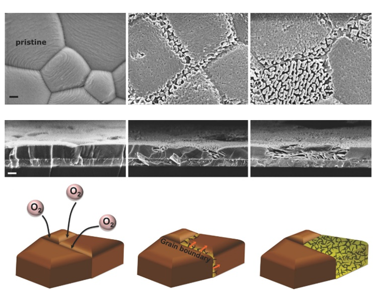
Adopted from Adv. Energy Mater. 2017, 7, 20, 1700977.
.
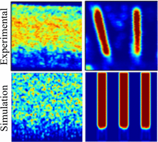
Ion migration and hysteresis: The mixed electronic-ionic nature of perovskite materials dictates that not only charge transport, but also ion transport takes place in perovskite materials. The transport of ions has been linked to the presence of hysteresis in perovskite photovoltaic devices and has been shown to increase their degradation. We investigate the migration of ions both experimentally and by numerical simulations in order to understand the fundamentals of this process and its effect on the performance and stability of perovskite devices.
Adopted from ACS Appl. Mater. Interfaces 2019, 11, 2, 2490-2499
.
Reproducibility: Perovskite devices are notoriously known to suffer from poor reproducibility. We investigate the various factors that influence the properties and performance of perovskite devices in order to develop more robust and reliable fabrication procedures.
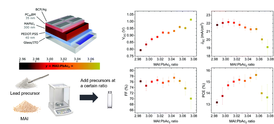
Adopted from Energy Environ. Sci. 2018, 11, 3380.
PbS Quantum Dots
Since their first introduction in 2008, lead sulfide (PbS) quantum dot (QD) photovoltaic devices have been under extensive investigation leading to record power conversion efficiency of 12.24%. One of the key advantages of quantum dots stems from their nano-character, which allows tuning their optoelectronic properties by choosing their size, shape and ligands. This multifunctionality has led to the realization that QDs can be used as both an active layer and as an extraction layer, providing appropriate ligands are selected. In particular, PbS QDs with 1,2-ethandithiol (EDT) ligands have become ubiquitously employed as a hole extraction layer in PbS quantum dot photovoltaic devices, including those with record efficiency, in which PbI2 ligands are used in the device active layer. Our work in the field of PbS quantum dot photovoltaics follows two main avenues:
Stability: A unique trait of quantum dot solar cells is that unlike other types of solution-processed devices, e.g. organic or organic-inorganic perovskite, quantum dot solar cells can experience an increase in performance upon exposure to the environment. Consequently, it has become routine in literature to perform preconditioning procedures, such as exposure to air prior to photovoltaic characterization, however the exact mechanism of this improvement remained unclear. Recently, we have identified that the improvement in performance stems from the difference in oxidation dynamics between quantum dots coated with different ligands. While PbI2-PbS dots show only minor changes in their composition and optical properties, the EDT-PbS quantum dots show a gradual decrease in size due to the formation of a shell of oxidation products. As a result, the increased bandgap of EDT-PbS enhances the efficiency of electron blocking by the EDT-PbS layer, drastically improving the device efficiency.
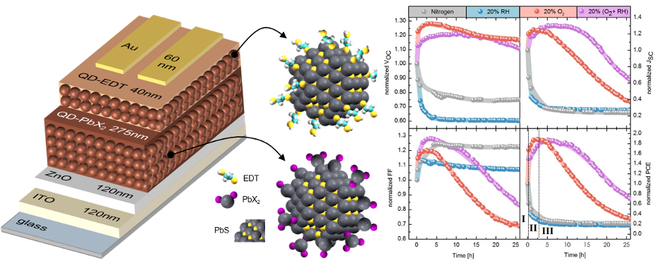
Adopted from Sustainable Energy Fuels 2020, 4, 108-115.
Perovskite-PbS core-shell structures: The excellent match between the atomic lattice constant of PbS and perovskites offers the possibility to synthesise a broad range of perovskite coated PbS quantum dots that are of interest for application in near-infrared absorbing photovoltaic devices. We investigate the role of perovskite shell composition on the properties, performance and stability of these devices. Recently, we demonstrated that triple cation perovskite shell is superior to the traditional methylammonium lead triiodide, resulting in a simultaneous enhancement in efficiency and stability.
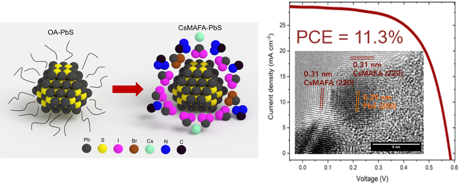
Adopted from ACS Nano 2020, 14, 1, 384-393.
Organic Semiconductors
Organic semiconductors have found application in a range of electronic devices due to the ease with which their properties can be tuned by synthesis. For example, organic light-emitting diodes are integrated into several technologies such as lighting arrays and displays. The field of organic photovoltaics has not yet fully been realised in industrial applications, but is currently experiencing a renaissance with remarkable advances in power conversion efficiencies recently reported for both single junction and double junction solar cells. Despite these major breakthroughs many aspects of device physics of organic solar cells, in particular those with low energy offsets, remain unknown. One of the most common aspects of the device is the energy level diagram (energetic landscape) of the solar cell, with such diagrams being ubiquitous in literature, appearing in almost every publication. Despite the importance of energy level diagrams in determining the elementary processes taking place in the device (e.g. charge generation, transport and extraction), accurately determining these diagrams is extremely challenging, especially for solution-processed systems. Currently, energy level diagrams are constructed by combining energy values for the individual components as obtained by different methods such as density functional theory, cyclic voltammetry, Kelvin probe and Ultra-violet photoemission spectroscopy (UPS), resulting in a large scatter in reported energy levels even for the same material systems. In addition, this approach neglects to account for interfacial effects such as formation of dipoles or band bending.
Recently, we have developed a new methodology to address this key challenge: a novel photoemission based technique that allows mapping of the energy level landscapes in various multi-layered devices with a superior vertical resolution of 1-2 nm. The technique is based on the combination of ultraviolet photoemission spectroscopy an essentially damage-free etching of materials in-situ using a gas cluster ion source. The new method has already been applied to a range of high performance photovoltaic systems, demonstrating both the efficacy and the versatility of the technique.
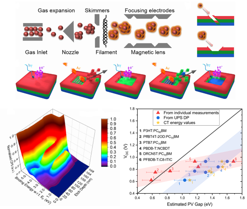
Adopted from Joule 2019, 3, 2513-2534.